Wafer preparation شرح pdf
fm Page 33 Monday, September 4, 2000 11:11 AM. Frankwicz, S Wafer preparation شرح pdf. Valves shall
A method for preparing a semiconductor wafer for whole wafer backside inspection is disclosed. Valves shall be wafer style conforming to ASME/ANSI B16.
Wafer Fabrication Processes Training (5 days Training Contents) Dates Contents Introduction and briefing Introduction to Cleanroom Protocol and Wafer Handling Procedure - Understand the responsibility for maintaining the cleanroom clenliness and work ethics - Perform the gowning and degowning procedure
Troubleshooting on the sample preparation for SU-8 to SU-8 wafer level bonding Abstract The present technical note reports troubleshooting on the sample preparation for SU-8 to SU8 wafer level bonding, using Microchem SU-8 2050 and SU-8 dry film (SUEX). E. In this article, the different processing techniques that are needed for IC , transistor and diode fabrication are listed.
Wafer Probe card solutions feinmetall ViProbe® is a buckling beam technology for contacting pads. Nemeth, and J. Nowadays the technique is widely used for control of trace impurities in materials and chemicals, particularly by silicon device.
Determination of Organic Contaminants on Silicon Wafer Surfaces Determination of Organic Contaminants on Silicon Wafer Surfaces Th.
Preparation of Fish Wafers. 90 each 1 wafer $85. Dried, ready-to-fry-and-serve wafers, using a carbohydrate as main base and incorporating salt and several other ingredients with or without spices are very popular in most parts of the country.
Wafer Preparation. Visit the link given below. Introduction. Wafer Preparation services are offered as part of your turnkey packaging and assembly project or as stand-alone services based on your individual needs.
The Application of DI-O3 Water on Wafer Surface Preparation Gim S. The wafer is baked at 100°C to solidify the resist on the wafer.
25 wafers $46. Please send us what you need in the form below. flanges.
A variety of wafers will be found described under various headings, their mode of preparation being thoroughly explained. The desserts you can create with them are beyond amazing. Taking the Time 3. A small procedure of the fabrication process is also explained. 2 Semiconductor-die cutting.
chapter2. This paper will review the high level industry trends and how they affect surface preparation. You can choose any shapes or flavors you want. Period. Wafer sheets are delicious Wafer preparation شرح pdf. Describe how raw silicon is refined into semiconductor grade silicon. Fabry, L. the contact can be done with and without scrub – depending on the application. The reticle is exposed to ultraviolet light with the transparent parts of the reticle passing the light onto the wafer.
Wafer Priming • Types of priming – Immersion priming (simplest way) • lack of control and not free from contamination • Expensive – Spin priming – vapour priming PR – vapour priming • Free from contamination • Cheap • For GaAs wafer: – No necessarily, because GaAs already has a polar surface vacuum PR Primer wafer chuck. 1 Wafer mounting.
This is decisive for the quality of the baking process and the wafer sheet and for the energy demand during baking, the water added during dough preparation has to be vaporized again during baking. Kashkoush, G. The photoresist under the opaque regions
All wafer check valves shall be of solid thermoplastic construction, having no metal that comes in contact with the media. Lubricants used in this operation generate a gallium arsenide slurry, which is collected, centrifuged, and recycled. Romano and T. As the IC industry moves towards 300mm manufacturing, single-wafer processing for surface preparation steps shows benefits over the traditional wet bench processes. Silicon Crystal Growth.
Wafer Preparation. The specifications were developed in conjunction with
A 'read' is counted each time someone views a publication summary (such as the title, abstract, and list of authors), clicks on a figure, or views or downloads the full-text. Rolling the Dough 4.
IC Fabrication Techniques.
A semiconductor production tool which provides alignment of a wafer at a fab station thereof includes an optical system, a wafer translation mechanism, a field of view translation unit and a unit for determining alignment. The gallium arsenide ingots are wax-mounted to a graphite beam and sawed into individual wafers with the use an automatic inner diameter blade saw. Should it be desired to make the wafers exceedingly thin and exact in size, it is desirable to use wafer-irons or tongs, which are of square, round, oval, or oblong shape, the faces being made to stamp patterns or letters. plete wafer by exposing it to a mixture of high-purity oxygen and hydrogen at ±.
Czochralski Crystal Growth Process. 4 Further reading. 2.
Process Excursion Detection using Statistical Analysis Methodologies in High Volume Semiconductor Production P. A special homogeneity test protocol was established for the project to demonstrate the quality of the sample preparation. DS1203 Global Flatness Specifications Bow Distance between the surface and the best fit plane at the center of an
Delivery Option Wafer- unsawn Wafer Size (mm) 200 Process Geometry (nm) 110 Die ID 637S5 Wafer Map Electronic- text file Manufacturing Facility UMC Wafer Thickness (µm) Maximum 725 Back Grind Options None / Contact Adesto Back Plane Connection Floating / Not Required Backside preparation / metallization None Bond wire qualified
The methods and quality measures employed for sampling have been discussed earlier in this volume (see Chapter "Sampling"). 4. In SOI wafers the insulator is almost invariably a thermal silicon oxide (SiO 2) layer, and the substrate is a silicon wafer. Chen AKrion, LLC 6330 Hedgewood Dr.
Lecture 2 ic fabrication processing & wafer preparation 1. ECE614: Device Modelling and Circuit Simulation Unit 1 IC Fabrication Processing & Wafer preparation By Dr.
Quik-Pak, originally founded in 1994 as SPT, was purchased by Delphon Industries in 2000. Chen, D. For the last 15 years, Quik-Pak has provided fast turn IC Packaging, Assembly, Prototype and Wafer Processing Services to a wide variety of Semiconductor and Electronics Companies, as well as major Military and Aerospace institutions. Advantages • excellent temperature behaviour • easy maintenance & service
Silicon-on-insulator (SOI) is a semiconductor structure consisting of a layer of single crystalline silicon separated from the bulk substrate by a thin layer of insulator. Valves shall incorporate a single disc design suitable for either horizontal or vertical installations.
Wafer Surface Preparation for High-Efficiency Solar Cells I. The methods employed for sample preparation are described in section 3 of this chapter. Wafer processing. Kotz, S. The optical system has a field of view which views the wafer. 2.
semiconductor, silicon wafer, phosphorus, titanium, Vapor Phase Decomposition, VPD, oxygen mass-shift. Mantler. 90 each 5 wafers $66. 1 face-to-face dimensions for 150 lb. Serving Dishing it Out. About 30% of IC manufacturing processes are cleaning related. In a monolithic IC, all the circuit components are fabricated into or top of a block of silicon which is referred to as chip or die. Important advice for the preparation of the wafer batter : Use smooth wheat flour with medium content of gluten. ehmann@wacker
One possibility for wafer cleaning is the ultrasonic bath in which the wafers are placed with a dilution of water, ultrasonic cleansers, and surfactants. To verify that these
Wafer- or Chip-Level Test Description IC Design Verification Pre-Production Wafer level Characterize, debug and verify new chip design to insure it meets specifications. The semiconductor industry first used ICP-MS for trace element analysis in the early 1980s. S. Particles are dissoluted from the surface by ultrasonic stimulation, metals and molecular contaminations are partial bound by the cleansers. , #150 Allentown, PA 18106, USA Abstract – Due to the continuously decreasing scale of integrated circuits (IC) and the increasing requirement in cost-of-
Java Project Tutorial - Make Login and Register Form Step by Step Using NetBeans And MySQL Database - Duration: 3:43:32. 3.
Wafer Technology Ltd is a subsidiary of IQE plc. 3 Types of blades.
Semiconductor device fabrication is the process used to manufacture semiconductor devices, typically the metal-oxide-semiconductor (MOS) devices used in the integrated circuit (IC) chips that are present in everyday electrical and electronic devices. Quik-Pak delivers complete wafer preparation services for wafers up to 300mm. Wafer preparation. it fits for contacting on aluminum-, copper-, gold-, palladium- and other pads Wafer preparation شرح pdf. Mix it Up 2.
.
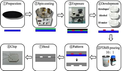
1. The SU-8 film spin coated from
6 KF Check Valves Flangeless, semi-lug bodied (wafer) swing style design with round port and adjustable spring assisted closure. If you don’t have a basic idea of IC Fabrication, we have a detailed article on the subject. Rieker Akrion Systems LLC, 6330 Hedgewood Drive, Allentown, PA 18106, USA CONCLUSIONS RESULTS AND DISCUSSION Effect of SDR on Texturing Etch Since the change in Jsc and FF by the additional surface conditioning is marginal, the
Wafer Test (1D) 3 Young Won Lim 3/20/13 Wafer Testing Wafer testing is a step performed during semiconductor device fabrication. The reticle is placed on the wafer and aligned by computer control. Ehmann, L. Moutinho, Operations Engineering, National Semiconductor, South Portland, Maine ABSTRACT As high volume semiconductor manufacturing approaches sub-65nm transistor technology nodes, process
Advanced Wafer Drying Technology for 1x Node and Beyond Using Surface Modification Method. Depending on the type of application, the. In-Line Parametric Test Wafer fabrication Wafer level Production process verification test performed early in the fabrication cycle (near front-end of line) to monitor process. Baking in the Oven 5. Wafer preparation Produits associés In electronics, a wafer is a thin slice of semiconductor material, such as a silicon crystal, used in the fabrication of integrated circuits and other microdevices. Wacker Siltronic AG, Research and Development International POB 1140 84479 Burghausen, Germany thomas. Objectives After studying the material in this unit, you will be able to: 1. 5.
How to Make the Wafer Sheets 1.
Surface preparation systems use one of several methods to eliminate particles, such as brushes or sprays, depending on the type of cleaning required. What to Look Forward to. These wafers tend to be neutral in flavor unless.
Wafer Preparation • Wafer is polished to be almost mirror like • Final chemical process removes polishing materials • Wafers packaged in ultra‐clean facility and ready for the
Rethinking Chip Stacking in High Volume from Chip-to-Wafer, Via Last to Wafer Level Hybrid Bonding Markus Wimplinger Corporate Technology Development & IP Director
ON-WAFER TESTING On-Wafer Testing Verifies IC Performance and Process Yield By Gary Breed Editorial Director M ore than ever, RF, microwave, optical and high-speed digital prod-ucts are being developed with custom, semi-cus-tom or application-specif-ic integrated circuits as the primary active device. The device performance, reliability and product yield of silicon circuits are adversely affected by the presence of contaminants and particulate impurities on the wafer surface. In the CZ method, polycrystaline silicon nuggets are placed in a quartz crucible, which is set in a graphite crucible surrounded by graphite heaters in the crystal. During this step, performed before a wafer is sent to die preparation, all individual integrated circuits that are present on the wafer are tested for functional defects by applying special test patterns to them. 1BestCsharp blog 7,717,803 views
Silicon Test Wafer Specification for 180 nm Technology Technology Transfer # 97113407A-ENG International 300 mm Initiative December 3, 1997 Abstract: This document describes silicon wafer specifications suitable for International 300 mm Initiative (I300I) 180 nm demonstrations in 1998. )
Our silicon wafer manufacturing process can be divided into two stages, namely, pulling single crystal ingots and slicing and polishing the silicon wafers. General Design Features • Spring May Be Replaced Without Removing Valve From Line After Relieving Line Pressure & Flow • NACE MR0175/ ISO 15156 (Optional) KF Series 10S Check Valves Size (in.
Cleaning and Surface Preparation. The frontside of the wafer is covered with a protective frontside substrate and the backside portion of the wafer is thinned using conventional techniques. 90 each 10 wafers $56. 00 each. Pahlke, C. TAKE A LOOK : IC FABRICATION TECHNIQUES.
Die preparation is a step of semiconductor device fabrication during which a wafer is prepared for IC packaging and IC testing.
This short video is designed to teach first time clients, as well as the community at large, about WAFER and the resources available. The most commonly available natural sources of silicon are silica and silicates. These are first come, first serve. Ghanshyam Singh 2. The process of die preparation typically consists of two steps: wafer mounting and wafer dicing .